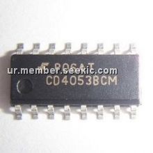
Product Summary
The CD4053BCM is a single 8-Channel multiplexer having three separate digital control inputs, A, B, and C, and an inhibit input. Each control input selects one of a pair of channels which are connected in a single-pole, double-throw configuration. The applications of the CD4053BCM include Analog and Digital Multiplexing and Demultiplexing, A/D and D/A Conversion, Signal Gating.
Parametrics
CD4053BCM absolute maximum ratings: (1)DC Supply Voltage (VDD): -0.5 VDC to +18 VDC; (2)nput Voltage (VIN): -0.5 VDC to VDD+0.5 VDC; (3)Storage Temperature Range (TS): - 65℃ to 150℃ ; (4)Power Dissipation (PD): Dual-In-Line, 700 mW; Small Outline, 500 mW; (5)Lead Temp. (TL) (soldering, 10 sec.): 260℃.
Features
CD4053BCM features: (1)Wide Range of Digital and Analog Signal Levels:Digital:3V to 15V, Analog to 15VP-P; (2)Low ON Resistance, 80Ω (Typ) Over 15VP-P Signal Input Range for VDD-VEE = 15V; (3)High OFF Resistance, Channel Leakage of ±10pA (Typ) at VDD-VEE = 10V; (4)Logic-Level Conversion for Digital Addressing Signals of 3V to 15V (VDD-VSS = 3V to 15V) to Switch Analog Signals to 15VP-P (VDD-VEE = 20V); (5)Matched Switch Characteristics, rON = 5Ω (Typ) for VDD-VEE = 15V; (6)Very Low Quiescent Power Dissipation Under All Digital-Control Input and Supply Conditions, 1μW (Typ) at VDD-VSS = VDD-VEE = 10V; (7)Binary Address Decoding on Chip.
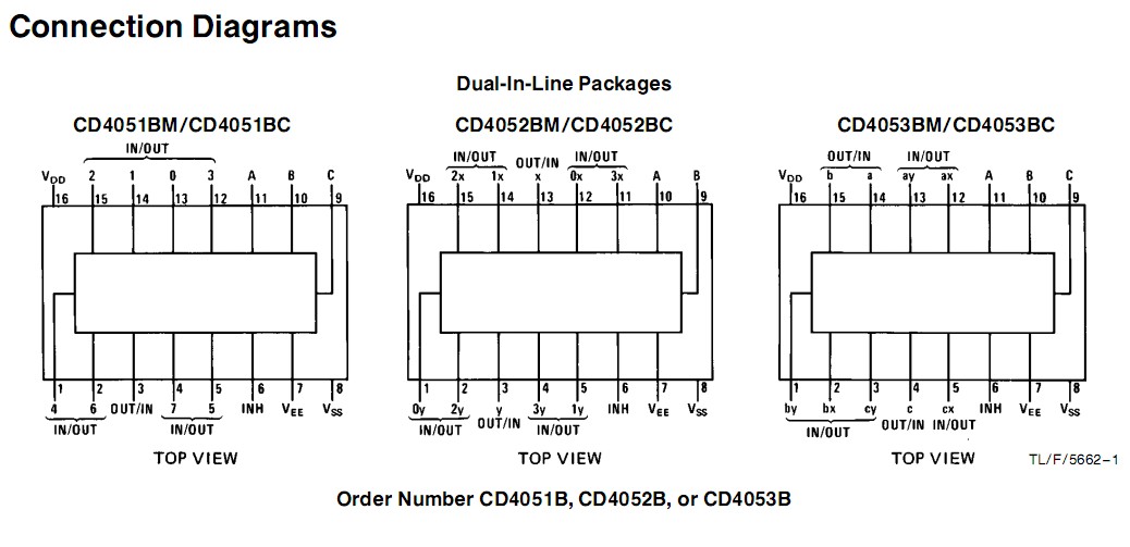
Diagrams
| Image | Part No | Mfg | Description |  |
Pricing (USD) |
Quantity | ||||
|---|---|---|---|---|---|---|---|---|---|---|
 |
 CD4053BCM |
 Fairchild Semiconductor |
 Multiplexer Switch ICs Multiplex/Demultiple |
 Data Sheet |
 Negotiable |
|
||||
 |
 CD4053BCM_Q |
 Fairchild Semiconductor |
 Multiplexer Switch ICs Multiplex/Demultiple |
 Data Sheet |
 Negotiable |
|
||||
 |
 CD4053BCMX |
 Fairchild Semiconductor |
 Multiplexer Switch ICs Multiplex/Demultiple |
 Data Sheet |
 Negotiable |
|
||||
 (China (Mainland))

