(China (Mainland))

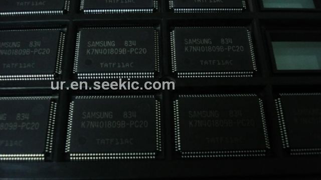
Product Summary
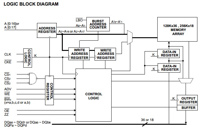
The K7N401809B-PC20 is 4,718,592 bits Synchronous Static SRAMs. Address, data inputs, and all control signals except output enable and linear burst order are synchronized to input clock. Write cycles are internally self-timed and initiated by the rising edge of the clock input. This feature eliminates complex offchip write pulse generation and provides increased timing flexibility for incomming signals. The K7N401809B-PC20 is implemented with SAMSUNG′s high performance CMOS technology and is available in 100pin TQFP packages. Multiple power and ground pins minimize ground bounce.
Parametrics
K7N401809B-PC20 absolute maximum ratings:(1)Voltage on Input Pin Relative to VSS:-0.3 to VDD+0.3V; (2)Voltage on I/O Pin Relative to VSS:-0.3 to VDDQ+0.3V;(3)Power Dissipation:1.4W;(4)Storage Temperature:-65 to 150°C;(5)Operating Temperature:Commercial,0 to 70°C/Industrial, -40 to 85°C ; (6)Storage Temperature Range Under Bias:-10 to 85°C.
Features
K7N401809B-PC20 features: (1)VDD=3.3V+0.165V/-0.165V Power Supply.; (2)Byte Writable Function; (3)Enable clock and suspend operation; (4)Single READ/WRITE control pin; (5)Self-Timed Write Cycle; (6)Three Chip Enable for simple depth expansion with no datacontention; (7)Α interleaved burst or a linear burst mode; (8)Asynchronous output enable control; (9)Power Down mode; (10)TTL-Level Three-State Outputs; (11)100-TQFP-1420A Package; (12)Operating in commeical and industrial temperature range.
Diagrams